In-situ optical measurement in a CMP tool is made through a window in the platen or polishing pad. Each time the rotating wafer passes over the optical window, broadband light is delivered to the wafer surface, the reflected spectrum is collected, and software extracts film thickness from the spectral reflectance data.
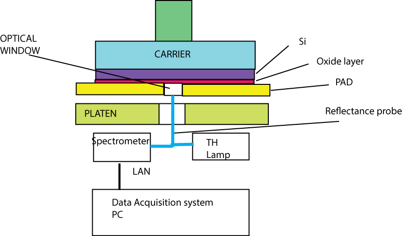
Continuous monitoring and endpoint detection
During oxide removal, interference fringes shift as the oxide thickness decreases and the reflectance trace changes smoothly. At endpoint, when the oxide clears and silicon or another layer such as SiN is exposed, the spectral signature changes abruptly. That change can be detected automatically while thickness is tracked in real time.
System architecture
- Broadband 5 W tungsten-halogen illumination source with 10,000 hour lamp lifetime.
- Ariel VIS spectrometer with 400–1000 nm wavelength range, high optical throughput and fiber-optic interface.
- Optical probe integrated under the CMP platen with illumination fiber, collection fiber, optical lens assembly and sapphire or quartz pad window.
- Real-time software for spectrometer control, spectrum acquisition, thickness tracking, data logging and customer software integration.
- Tool interface through Modbus TCP server or DLL API library.
Measurement rate in the CMP environment
The measurement interval is limited by rotation, and it is often useful to take multiple measurements within one rotation to sample different wafer locations. The measurement has two parts: data acquisition and data analysis. Acquisition time is set by signal strength; the Ariel spectrometer minimum integration time is 10 µs, while a typical CMP environment may require about 5 ms because slurry and window contamination reduce signal.
| Condition | Typical time |
|---|---|
| Minimum spectrometer integration time | 10 µs |
| Typical integration time on Si | ~1–2 ms |
| Typical integration time in CMP environment | ~5 ms |
| Thin-film data analysis, < 1 µm | < 100 ms |
| Thick-film data analysis, > 1 µm | < 10 ms |
For maximum measurement rate, data acquisition and data analysis can be separated: acquisition proceeds at the maximum rate allowed by signal strength, while analysis runs separately on a calculation server and only measurement results, such as thickness, are sent to the data server.
Why broadband reflectometry
Broadband spectral reflectometry provides continuous thickness measurement and stack sensitivity in addition to clear endpoint detection. It is especially useful for oxide thickness monitoring, dielectric CMP, R&D work and advanced-node process development where multilayer sensitivity matters.