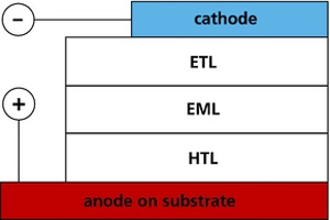
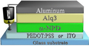
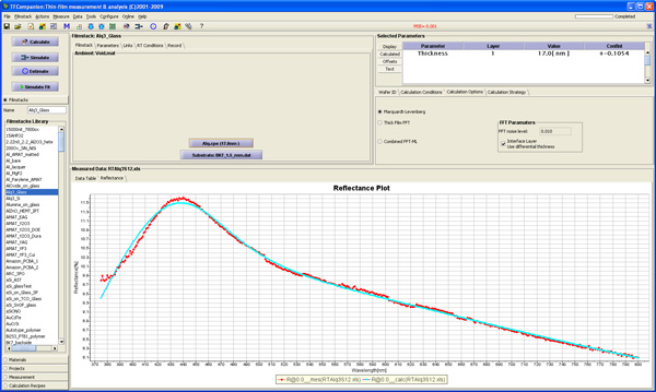
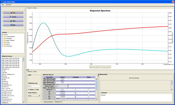
OLED structures stack several thin organic layers between electrodes, and both thickness and optical constants must be measured and controlled in R&D and production. MProbe 20 UVVis is well suited; for patterned samples, small-spot measurement on a pixel uses MProbe 40 UVVis. A common implementation uses NPD (hole transport) and Alq₃ (electron transport), both with complex UV dispersion that depends on deposition - Alq₃ especially, as it has several crystalline phases.
Very thin layers (< 10 nm) are measured easily, and because most organic materials have UV absorption structure, optical dispersion can be determined even on thin layers. The same filmstacks and approach transfer between R&D and production, with inline or in-situ work typically using the MProbe UVVisF variant.
Why use MProbe UVVis?
- Very thin layers (< 10 nm) are measured easily.
- Most organic materials have electronic transition/absorption structure in the UV region, making optical dispersion measurable even on thin layers.
- Complex materials such as Alq₃ can be checked for both optical constants and thickness.
- The same filmstacks and measurement approach can transfer from R&D to production.
- Inline and in-situ measurements typically use the MProbe UVVisF version.
Basic specification
| Recommended system | MProbe 20 UVVis; MProbe 40 UVVis for small-spot patterned samples |
| Wavelength range | 200–1000 nm |
| Wavelength resolution | 2 nm typical, depending on spectrometer slit |
| Measured thickness range | 1 nm–75 µm |
| Precision | < 0.01 nm or 0.01% |
| Spot size | < 1 mm; see MProbe 40 UVVis for smaller spot sizes |
| Light-source lifetime | 2000 hr; for longer lifetime see MProbe UVVisF |
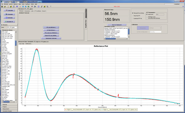
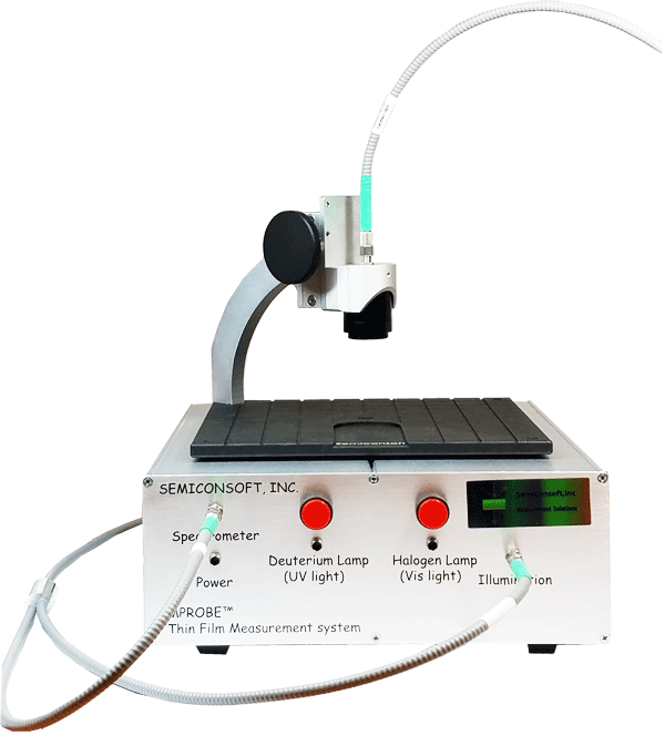
Measured with: MProbe 20 / 40 UVVis (MProbe UVVis).